
When we founded Ouster in 2015, our experience building lidar sensors at Quanergy gave us a uniquely informed perspective on how to design a lidar sensor. At any given point in time, the market always demands a sensor that is high performance, reliable, and affordable, but what is critically overlooked is that meeting market demands at a given point in time is not enough to win a maturing industry. The lidar industry is a rapidly maturing and changing landscape, with ever-increasing performance and cost needs. What we realized back in 2015 was that the long-term winners in the lidar industry need to do more than meet the current demands of customers. The long-term winner will meet the demands of the day, and also have the headroom to steadily improve performance and cost over time to keep pace with the needs of customers. It’s with this insight in mind that we invented digital lidar technology.
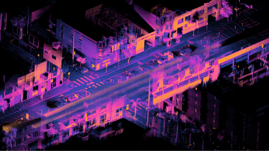
A lidar pointcloud of Folsom Street in San Francisco taken by a car with Ouster sensors mounted on it.
Our patented digital lidar technology delivers high performance, reliability, and affordability today, and critically, our CMOS approach enables us to steadily improve our performance for many years to come. In this post, we’ll go deeper than we ever have before into what makes our digital lidar technology unique and how we brought the power of Moore’s Law to lidar.
Ouster’s Digital Lidar Architecture: Simple Yet Powerful
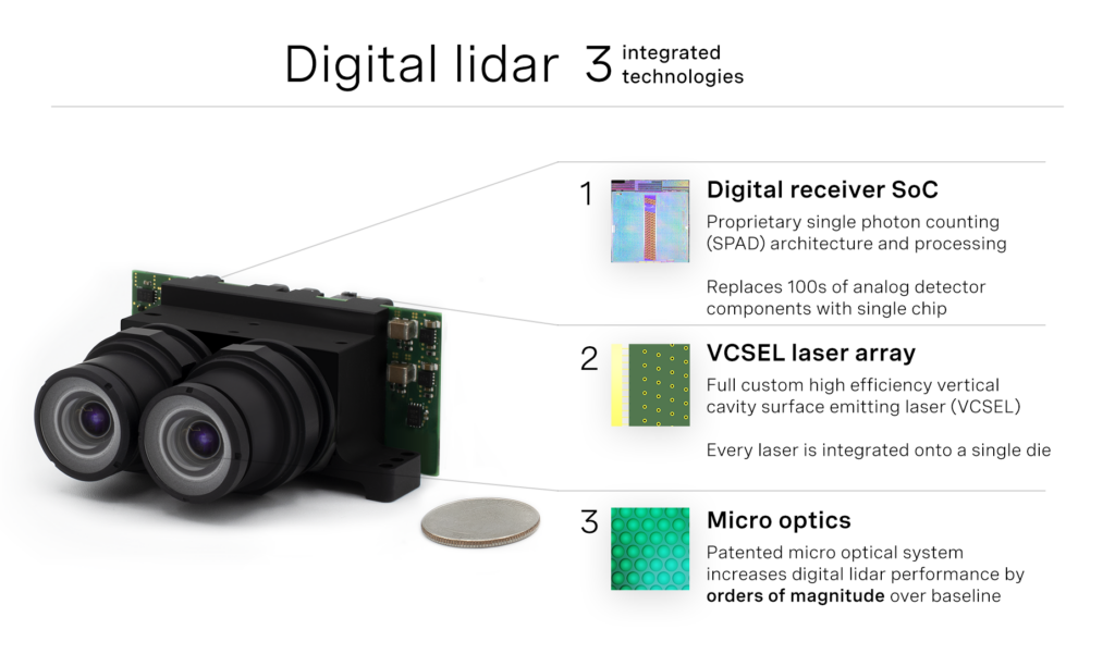
All of Ouster’s sensors are built on the same core digital lidar technology – a simple two-chip architecture that replaces hundreds to thousands of discrete components commonly found in traditional analog lidar. Our system consists of three integrated technologies, two chips, and one set of micro optics:
- custom system-on-a-chip (“SoC”) with single photon avalanche diode (“SPAD”) detectors
- vertical cavity surface emitting laser (“VCSEL”) array
- patented micro-optical system
VCSELs and SPADs are broadly deployed in non-lidar markets: smartphones (FaceID on iPhones, for example), medical equipment, telecom infrastructure, and more. The technology, though relatively new, is used in these industries because it is low cost, easily mass produced, and reliable. The reason it wasn’t used in lidar was because no one had solved how to meet the performance specs, namely range, of the high-resolution lidar market. Based on the current state of the art back in 2015, a lidar sensor built with VCSELS and SPADs would have a range of only a few meters – not nearly enough to be a viable solution. But the core components , VCSELs and SPADs were rapidly improving.
What we saw back in 2015 was an opportunity to design a lidar sensor that could ride a wave of innovation in VCSEL and SPAD technology, combined with one of our key breakthroughs: new micro-optics that use light more efficiently, to build a high-resolution digital lidar that could meet customers’ required specifications.
The result of our work is a low-cost integrated digital lidar sensor. Because VSCELs and SPADs have improved in the intervening years, we have sensors today that are affordable, highly reliable, have the highest resolution available, are capable of 200+ meter range, and have many years of improvement ahead.
digital lidar integrated technologies
Custom SoC With SPAD Detectors
This System-on-a-chip, or SOC, is developed in-house and mass-produced in a standard silicon CMOS process. It counts over 1 trillion photons per second with a natively digital output (1s and 0s for whether a photon was detected), and also handles the logic and signal processing that runs the sensor. Because SPADs have single photon sensitivity, low noise, and extremely good timing resolution (jitter is typically between 10 ps and 100 ps), they are able to detect and timestamp the ultra-short laser pulses in our lidar. This sensitivity makes our SoC capable of detecting relatively weak laser light pulses from long range targets.
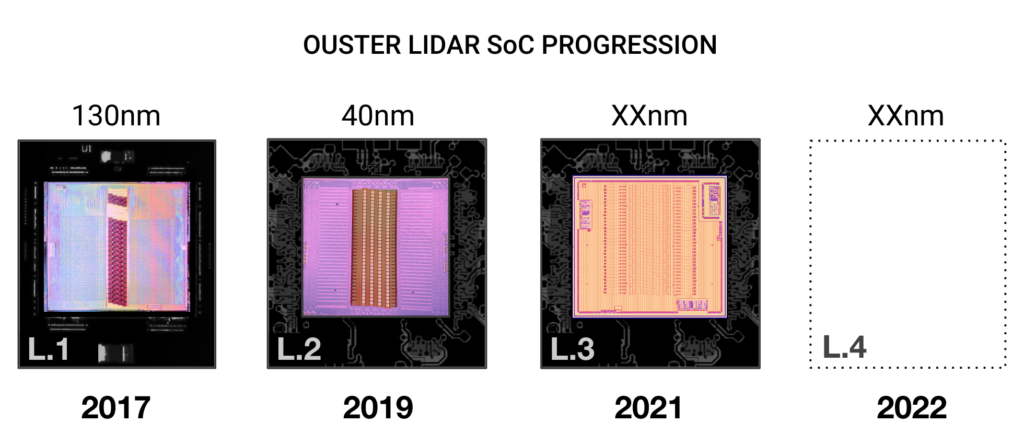
Ouster Lidar SoC Progression
With all the advantages of SPADs, it’s important to also highlight one key drawback of using SPADs today – low photon detection probability (“PDP”). Photon detection probability is a metric of efficiency used for light sensors that describes a sensors’ probability of registering a return when hit with an individual photon. Analog lidar detectors, Avalanche Photodiodes (“APDs”), are a mature technology with no major expected improvements in detection efficiency. SPADs on the other hand, may suffer from low PDP today, but there is significant room for improvement and a tremendous amount R&D investment to make it happen. Our sensors achieve up to 200 meter range today, and as SPAD technology improves, that range will continue to increase.
Pushing VCSEL Performance to the Limit
The second key component in our digital lidar sensors is an array of VCSELs. We use VCSELs because they are smaller, lighter, more durable, faster, and more cost efficient than edge emitting lasers used in analog lidar devices. The key physical and economic advantage of VCSEL technology is the ability to pack many lasers into a dense array. The array on our current sensors packs 128 lasers into an area the size of a grain of rice. Importantly, the cost of VCSELS does not increase linearly with each additional laser. This density gives us high-resolution and low cost in a small form factor today, with plenty of headroom to add more resolution without increasing the size of our sensors.
Increasing Performance With Micro-Optics
The third component is our patented micro-optics, which enhance the performance of both our emitters and detectors. This optical layer efficiently directs light through our lidar sensor, increasing detector efficiency by multiple orders of magnitude. This efficiency gain is key to the performance of our sensors, but we’ll come back to this shortly.
One Module to Rule Them All
Our SoC, VCSELs, and micro-optics are the basis of every sensor that we produce. These common components form a foundational lidar unit that can then be customized for different fields of view, ranges, resolutions, or even into a solid-state sensor.
Ouster's digital lidar optical module help the OS0, OS1, OS2, and ES2 be configured into 75+ unique configurations
Just as we are accustomed with DSLR cameras, different lenses afford us the ability to use common sensing components and swap lenses to customize our products for different uses. Our OS0 and OS1 units, for example, have the same form factor and core sensing components, but use different optics. With this easy customization, we are able to unlock cost reduction in our supply chain while delivering two distinct products that can better fit the needs of our diverse customer base.
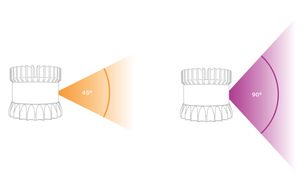
Ouster sensors with 45 or 90 degree field of view
Legacy Analog Lidar: The Performance and Cost Tradeoff
Compared to Ouster’s simplified digital lidar architecture, analog lidar contains hundreds of discrete parts, making it inherently complex and with little room for future performance improvements.
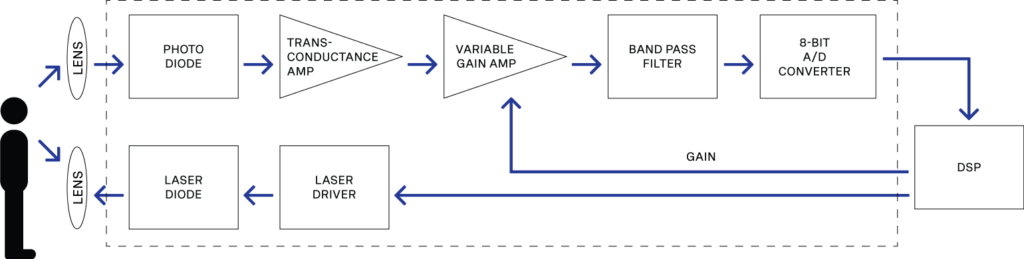
Analog lidar flow chart
Above is a diagram from a foundational patent of analog lidar, which shows all the components of a single channel of resolution. The component count scales linearly with resolution – adding one channel of resolution requires the addition of 1 emitter PCB, 1 edge emitting laser, 1 laser driver, 1 receiver PCB, 1 receiver APD, 1 ADC, and a dozen more parts.
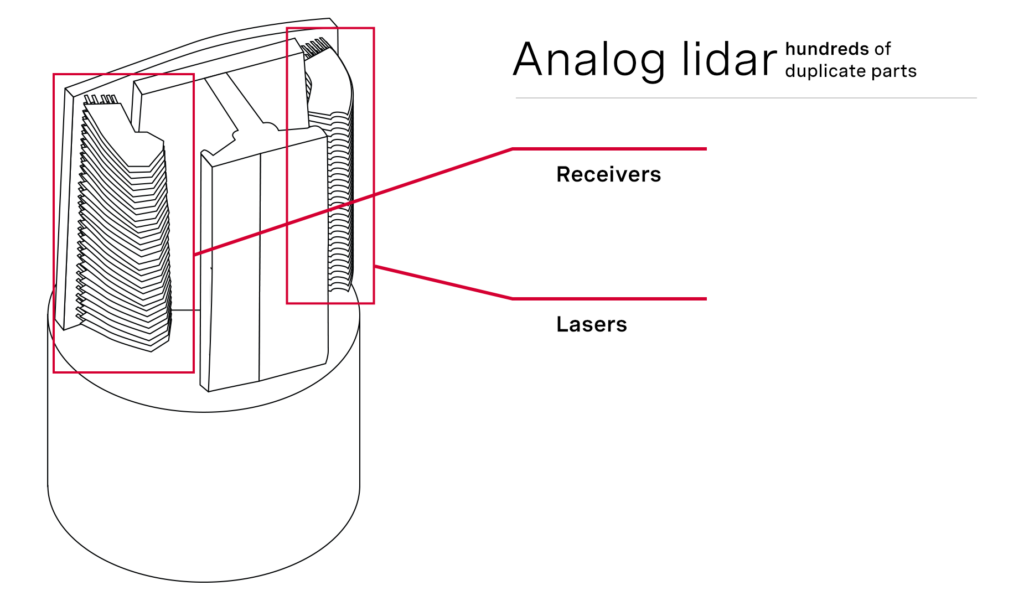
Analog lidar has hundreds of duplicate parts
To create a functioning analog sensor, these boards are stacked in a device as you can see above. This is a 32-channel spinning lidar. Increasing resolution to even 32 channels increases the technical and mechanical complexity extremely quickly – simultaneously inflating cost and reducing reliability.
Analog’s complex architecture is the biggest limitation when it comes to performance and efficiency improvements. Increasing the number of components leads to higher costs, a bigger and heavier sensor, and lower reliability due to added potential points of failure.
For a deep dive of how digital lidar compares, you can watch our Digital vs. Analog Lidar Webinar.
MEMS: A Micromechanical Bottleneck
Another approach to lidar that we commonly see in the market is the use of MEMS mirrors, which promises improved reliability, though faces similar scalability issues to analog lidar. The promise of MEMS mirrors is improved reliability through the use of very small moving mirrors to steer the laser beams. The true reliability improvement of MEMS sensors remains to be proven, as even small mirrors are subject to issues of shock and vibration. That said, longer term, the bigger issue for MEMS-based approaches is future avenues for performance improvement.
In order to increase resolution, MEMS makers must add additional lasers to their lidar system. With a single very small mirror, adding additional lasers becomes a physical challenge, as you can see in the image below. Beyond a small handful of lasers, the only way to further increase resolution is duplicate the entire MEMS/laser unit within your system. This approach is being taken by MEMS makers in the market, but both cost and reliability will suffer as the number of components increases linearly with the increased resolution.
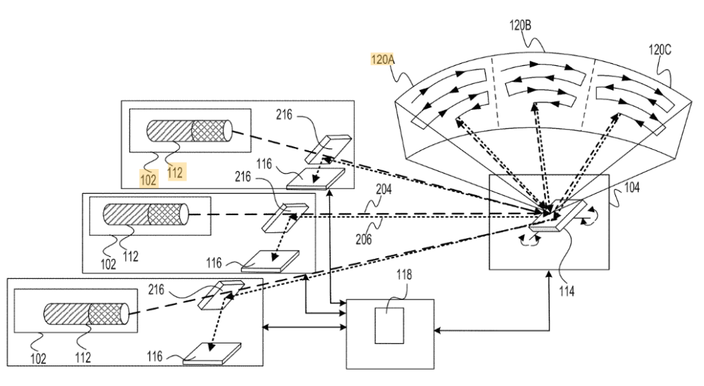
Source: https://patents.google.com/patent/US10107915B2/
Source: https://patents.google.com/patent/US10107915B2/
1550nm Sensors: The Brute Force Approach to Range
There are two approaches to achieving long range in a lidar sensor: brute force via a powerful laser, or increased efficiency via a more sensitive detector. Today in the market, there are a number of players who have adopted powerful 1550 nm lasers, taking a brute force approach to lidar performance. When operating at this wavelength, lasers can be pulsed with significantly more power and still remain within the eye safety limit.
Higher power enables a sensor to detect objects that are a greater distance away, but critically, these systems are missing the performance improvement curve afforded by a CMOS-based approach. The primary innovation will be in the realm of cost reduction. We see this at play with entrants into the market developing systems using silicon photonics. Companies are using silicon photonics to integrate 1550 nm systems “on a chip,” but the benefit of this integration are one-time gains. In order to further increase resolution or range over time these systems will have to be redesigned from the ground up using a different technical approach.
Looking Ahead: Commitment to Continuous Improvement
Digital lidar is built on the idea that if you can consolidate all of the important functionality of a lidar sensor into semiconductors fabricated in a standard CMOS process, you can put your core technology on a radically different price/performance improvement curve than is possible with other analog, MEMS, or silicon photonics-based approaches.
At this point you may be asking, if using SPADs and VCSELs has all of these performance and cost advantages, why doesn’t everyone use them? The short answer is that it’s really hard to make them work. Back in 2015 when we first began down the path of digital lidar, the current state of the art detectors and lasers would have produced a sensor with a range of only a few meters. Today, our OS2 has a range of over 200 meters and will continue to improve significantly over time. Crucially, its cost – and the cost of all our sensors – will come down at the same time.
At Ouster, we envision a future where lidar-powered solutions are ubiquitous, with high-performing and affordable 3D perception capabilities built for every industry. We are convinced CMOS digital lidar technology is what will get us there.
To learn more about our digital lidar technology: