Silicon eats industries. Lidar is next.
Our team has fielded a lot of questions in the past year asking how Ouster has been able to achieve such incredible performance in such a compact, low cost form factor. I’m excited to announce that Ouster has been granted foundational patents for our multi-beam flash lidar technology which allows me to talk more openly about the incredible technology we’ve developed over the last three years and why we’re going to lead the market with a portfolio of low-cost, compact, semiconductor-based lidar sensors in both scanning and solid state configurations.
I’d like to use the rest of this post to dive deeper into what’s behind the orders of magnitude performance improvements that we’ve achieved, and why it’s the most likely technology to go in every car – and every outdoor robot – of the future. Stick around – this is going to get technical!
An Unusual Operating Wavelength
While our technology is applicable to a wide range of wavelengths, one of the more unique aspects of our sensors is their 850 nm operating wavelength. The lasers in a lidar sensor must overcome the ambient sunlight in the environment in order to see obstacles. As a result lidar engineers often choose operating wavelengths in regions of low solar flux to ease system design. Our decision to operate at 850 nm runs counter to this trend.
A plot of solar photon flux versus wavelength at ground level (the amount of sunlight hitting the earth versus wavelength) shows that at 850 nm there is almost 2x more sunlight than at 905 nm, up to 10x more sunlight than at 940nm, and up to 3x more sunlight than 1550 nm – all operating wavelengths of legacy lidar systems.

We’ve gotten plenty of strange looks for our choice given that it runs counter to the rest of the industry. However, one of our patented breakthroughs is exceptional ambient light rejection which makes the effective ambient flux that our sensor sees far lower than the effective flux of other lidar sensors at other wavelengths, even accounting for the differences in solar spectrum. Our IP turns what would ordinarily be a disadvantage into a number of critical advantages:
- Better performance in humidity: Water vapor absorption in the upper atmosphere causes the helpful dips in the solar spectrum at 905, 940, and 1550 nm, but the same effect absorbs precious laser energy in humid and foggy conditions at ground level when the laser pulses transmit through the air resulting in less laser light captured by the lidar receiver. By contrast, the 850 nm spectrum has lower atmospheric water vapor absorption in all conditions – as much as several orders of magnitude better than other popular lidar operating wavelengths like 1550 nm. This means our lasers aren’t absorbed in humid condition and we achieve more consistent operation overall. Water vapor absorption issues shouldn’t be confused with liquid water in the atmosphere like rain, or dense fog which are challenging but surmountable conditions for all lidar sensors.
- Improved sensitivity in CMOS: Silicon CMOS detectors are far more sensitive at 850 nm than at longer wavelengths. There is as much as a 2x reduction in sensitivity just between 850 and 905 nm. Designing our system at 850 nm allows us to detect more of the laser light reflected back towards our sensor which equates to longer range and higher resolution.
- High quality ambient imagery: We recently released firmware that allows the OS-1 to collect ambient imagery in addition to lidar images, and the 850 nm operating wavelength has much to do with this. With more photons from the sun to collect at 850 nm, the imagery has higher signal to noise ratio and is more usable at dawn, dusk, or on cloudy days.
- Access to lower power, higher efficiency technologies: While more a result of our ambient light suppression than the 850nm spectrum specifically, our IP has allowed us to lower the ambient “noise floor” at any operating wavelength by more than an order of magnitude compared to our competitors. This allows us to use a variety of low power, high efficiency technologies in the laser and receiver that were traditionally considered impossible to incorporate into a high performance lidar (more on this in a bit). Ouster’s technology is focused on doing more with less – less cost, less power, smaller size, and fewer components.
And since we’re asked about it occasionally, the lasers we use are well under the eye safety limit and have been certified as Class 1 eye-safe lasers by third party labs.

Multi Beam Flash Lidar with SPADs and VCSELs
One of the most consistent pieces of feedback we’ve gotten from customers (some of which have tried and failed to develop their own lidar systems) is their surprise that we achieve such high performance with an all semiconductor approach that leverages a unique laser-detector combination: vertical cavity surface emitting lasers (VCSELs) and single photon avalanche diodes (SPADs). VCSELs and SPADs are cutting edge laser and detector technologies that are broadly deployed in markets outside of lidar – they are in smartphones, optical mice, medical equipment, telecom infrastructure, and more – but until now there have been insurmountable challenges to using them in high resolution lidar systems.
As far as we are aware, Ouster is the first company to not just demonstrate but also commercialize a combination of long range and high resolution sensing with VCSELs and SPADs in all ambient conditions.
There’s a reason for this – it’s super hard.
While there are multiple spinning lidar companies using side emitter diode lasers and APDs, multiple FMCW/doppler lidar companies using telecom style fiber optics and frequency tunable lasers, multiple 1550 nm galvo scanning lidar companies using fiber lasers, and multiple MEMS scanning lidar companies, Ouster is the first company to commercialize a high performance SPAD and VCSEL approach.
Explaining “Multi-Beam Flash” Lidar
Over the last three years, we’ve developed IP to solve the issues that kept these single chip technologies out of lidar previously, culminating in the multi-beam flash lidar architecture that plays to the strengths of VCSELs and SPADs. In this case, “flash” refers to the idea that every pixel in the sensor is illuminated by the laser and actively collecting light simultaneously like a camera with a flash, and “multi-beam” refers to the fact that the scene is illuminated with precision beams of light instead of a flood.
This second point goes back to Ouster’s focus on efficiency: the flood illumination in a conventional flash lidar, while simpler to develop, wastes laser power on locations the detectors aren’t looking. By sending out precision beams only where our detectors are looking, we achieve a major efficiency improvement over a conventional flash lidar.
In addition, VCSEL’s aren’t as bright (yet) and SPAD’s aren’t as efficient (yet) as the high cost legacy technologies currently employed, but what each lacks in raw performance they make up for in virtually every other metric: reliability, durability, low noise, high temperature operation, electrical efficiency, compactness, cost, direct integration with peripheral components, massive peripheral R&D activity driven by the consumer electronics industry, and equally massive room for fundamental performance improvements.
This last point is incredibly important – unlike other technologies, VCSELs and SPADs will realistically improve in fundamental performance by 10x each, and Ouster is at the forefront of this effort, investing in R&D in conjunction with partners to improve the core characteristics of these devices. With our technology, compact lidar sensors with HD resolutions are on the horizon.

Pushing VCSEL Performance to the Limit
We use VCSELs because they are smaller, lighter, more durable, faster, simpler to fabricate, and more power efficient than other laser technologies. While some types of pulsed lasers used in lidar systems today (e.g., 1550 nm fiber lasers) can cost thousands of dollars and draw tens or hundreds of watts of electrical power, our VCSELS are orders of magnitude cheaper and consume single digit watts of power in a tiny form factor. They’re also on a Moore’s Law-esque improvement curve in terms of performance, volume, and cost with hundreds of billions of VCSELs shipped worldwide to date.
At the same time, our VCSELs look nothing like those used in an optical mouse or a smartphone. We’ve developed custom VCSEL modules that combine all lasers on a single semiconductor die, and we’ve made breakthroughs at every level of the design to increase VCSEL effective brightness by orders of magnitude, while also narrowing their light pulses down to a few nanoseconds.
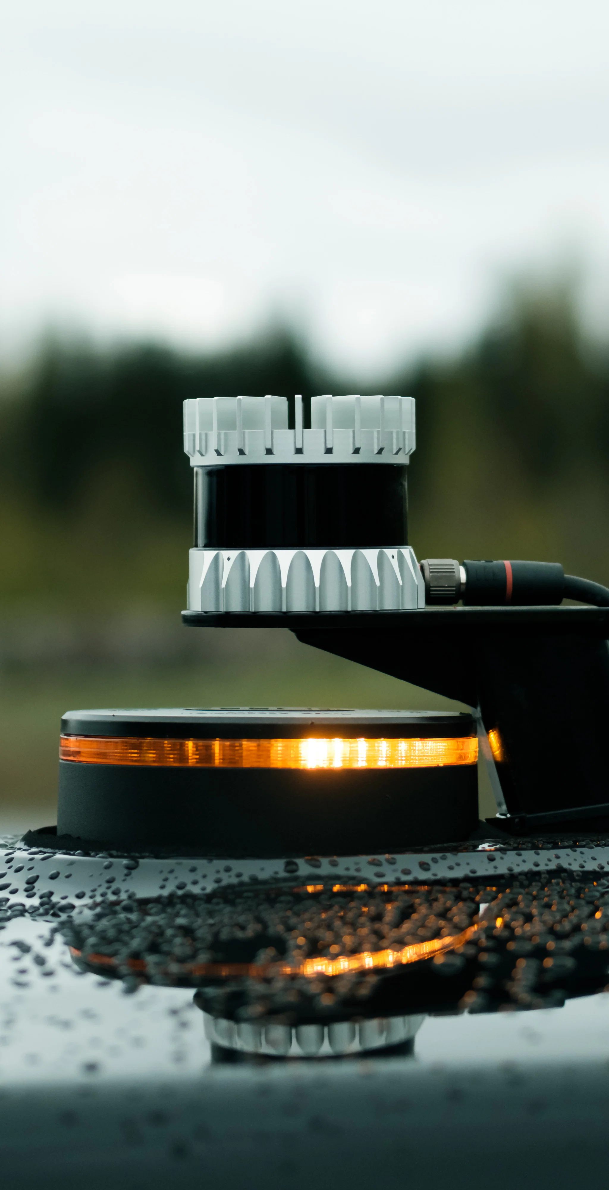
Our single VCSEL die has the added advantage of massively reducing system complexity and cost. Where other lidar sensors have tens or even hundreds of expensive laser chips and laser driver circuits painstakingly placed on a circuit board, Ouster sensors use a single laser driver and a single laser die. A sliver of glass no bigger than a grain of rice is all that’s needed for an OS1-64 to see 140 meters in every direction. It’s an incredible achievement of micro-fabrication that our team has gotten this to work at all, let alone so well.
A Novel CMOS ASIC with SPAD Detectors
The second chip in our flash lidar is our custom designed CMOS detector ASIC that incorporates an advanced single photon avalanche diode (SPAD) array. SPADs are a relatively new type of photo sensor that creates a binary pulse when a photon is detected as opposed to a traditional camera pixel which generates an analog signal that varies continuously with the amount of light on the detector. SPADs have single photon sensitivity, low noise, and extremely good timing resolution (jitter between 10 ps and 100 ps is typical. That’s picoseconds – mere trillionths of second!), all of which make them perfect for detecting and timing the ultra short laser pulses in our lidar.
Like VCSELs, CMOS SPADs have many practical advantages over the traditional approaches from other lidar manufacturers. Most important is that they can be directly integrated in a CMOS wafer, which makes it possible to incorporate massive amounts of signal processing on the silicon die right next to the detectors.
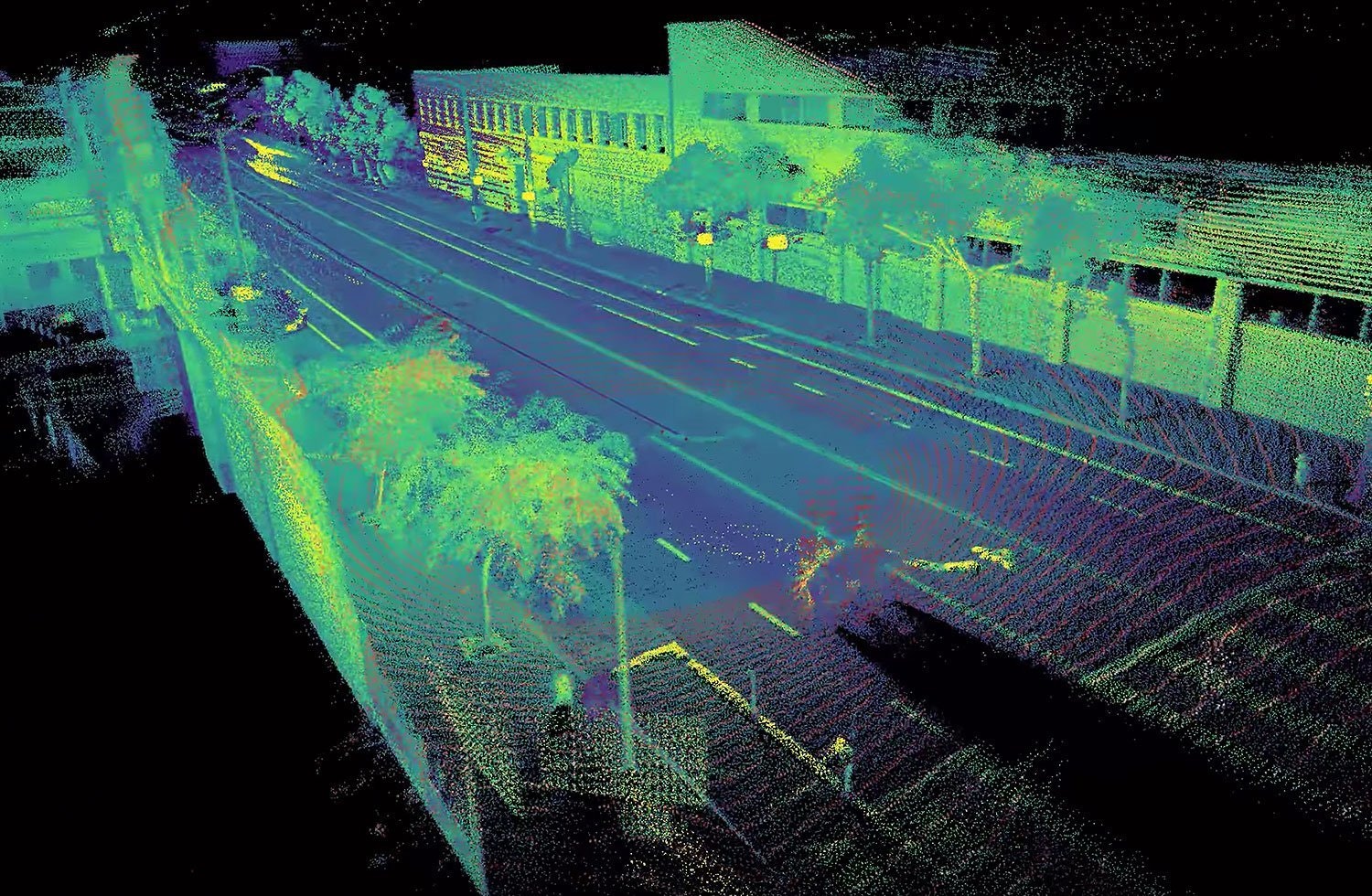
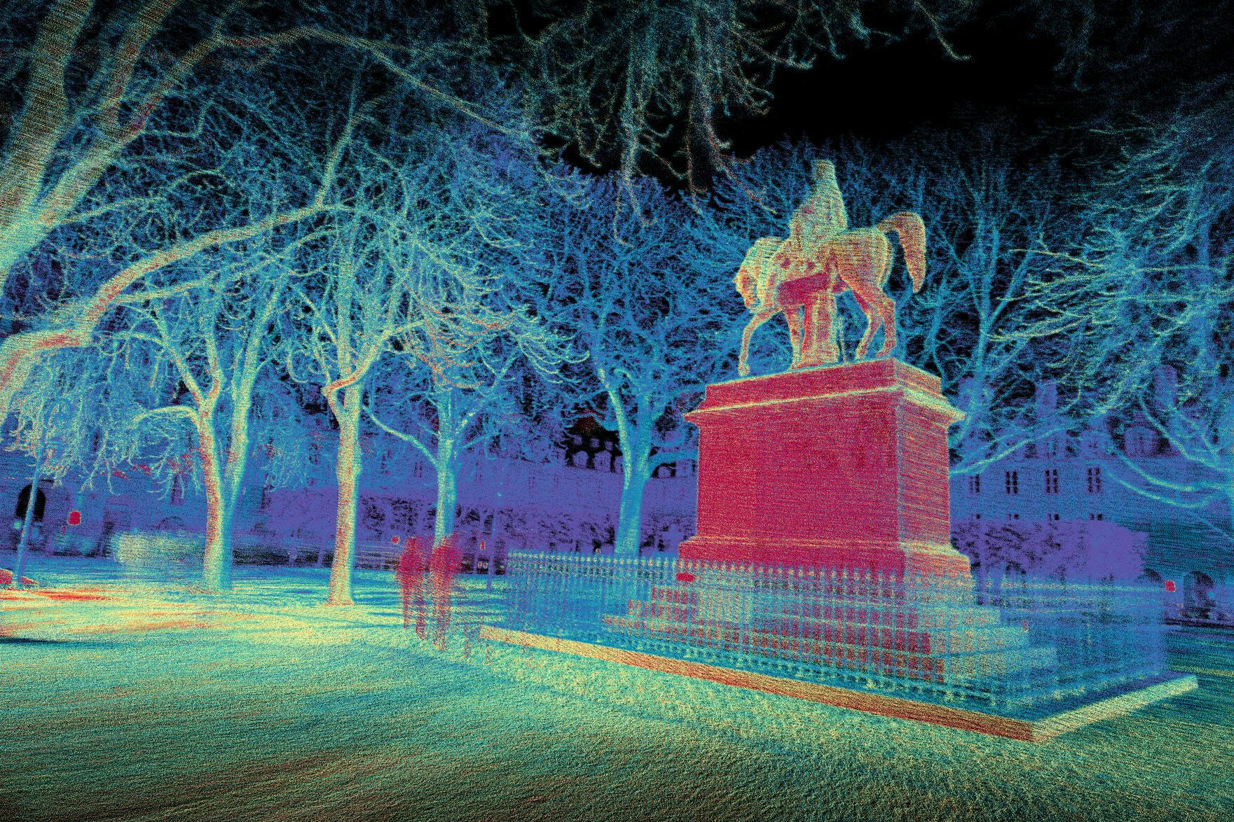
As lidar resolutions and data rates continue to increase, on-chip signal processing is essential – the current OS1-64 detector is capable of counting and storing over one trillion photons per second into on-chip memory. This is a titanic amount of data, and we’ve included over 100 GMACs per second (1 GMAC = 1 billion multiply accumulate operations) of signal processing logic in over 10 million transistors to ultimately produce the millions of 3D points per second that our customers use to drive cars, map environments, and identify obstacles.
Processing requirements are only going to go up, and Ouster is leading the way with our custom silicon.
SPADs are also moving along a Moore’s Law-esque performance curve. While today’s SPADs might be 2-5% efficient (efficiency here is measured as the percentage of photons that hit the detector that trigger a binary pulse. Most photons travel through the silicon without causing a pulse to trigger which is a bummer), new SPADs are 20-30% efficient (at 850nm) and efficiencies up to 80% may be possible as the technology matures. Increases in SPAD detector efficiency directly increase a sensor’s range and resolution – a 10x efficiency increase makes an OS1 with 640 lines of resolution not just possible but extremely likely. Unlike the legacy detector technologies used in lidar, our SPAD technology already achieves market leading performance but there is more than an order of magnitude improvement still left to go.

High Stakes Silicon
Developing our own ASICs is key to our breakthrough performance and cost, but the approach is not without risk. Each ASIC tape out – a “tape out” is an industry term for producing a set of unchangeable, high cost lithographic masks that are used in production of the wafers – is a multimillion dollar investment with lead times measured in quarters or years. Errors in a design can and do happen and often times cannot be fixed – there’s no such thing as recompiling your ASIC!
In our first three years, a mistake with a tape out could have ended the company, but Ouster’s ASIC team has distinguished themselves time and again and they’ve now delivered seven successful ASICs – each more powerful, more reliable, and more refined than the previous. Our team’s execution in this high stakes environment has paid off immensely, but we don’t take it for granted.
Our Way to the Highway
Ouster has successfully commercialized the first multi-beam flash lidar using VCSELs and SPADs through a strategic choice of operating wavelength, fundamental breakthroughs in ambient light suppression, and tightly integrated custom VCSEL and SPAD arrays. With our unique approach we’re able to deliver a more robust, higher quality 3D sensor at a lower retail price and lower bill of materials than any other company on the market.
With over a dozen additional patents pending, we’re doing more than building interesting technology and performant products – we’ve positioned ourselves as a technology leader in the competitive lidar market.
Writing about our technology is great, but shipping performant products is far more satisfying. Our sensors are shipping now and being used by hundreds of customers across a wide variety of industries including automotive, autonomous vehicles, robotics, mapping, security, and UAVs.
If we can help with your 3D sensing needs, reach out to us – we’d love to tell you more!


